The big picture: Taiwan’s E&R Engineering is fully committing to glass substrates for advanced packaging. Late last month, the company hosted an event in Taipei to launch its new “E-Core System” initiative, which also established the “Glass Substrate Supplier E-Core System Alliance.” The program aims to bring glass substrates into the mainstream for next-generation chips and high-speed communication devices.Industry coalition aims to make glass substrates the standard in chipmaking
The alliance brings together several key players, including German firm Manz AG, Taiwan’s Scientech for wet etching, Hyawei Optronics for AOI inspection, as well as Lincotec, STK Corporation, Skytech, and Group Up for sputtering and ABF lamination equipment. Several other component suppliers are also part of the coalition.
You can read more Technology articles
The combined expertise will enable the E-Core Alliance to deliver end-to-end glass substrate solutions to customers both globally and within Taiwan’s semiconductor industry.
In chipmaking, substrates form the foundation
upon which the integrated circuit is built. They provide a base material onto which various thin-film layers, such as semiconductors, insulators, and metal interconnects, are deposited and patterned using lithography and etching techniques. The choice of substrate material significantly impacts the chip’s performance, reliability, and manufacturing costs.
Compared to copper, glass substrates offer denser wiring, faster signal transmission, extreme flatness, and the ability to withstand high heat and voltages. These properties make glass ideal for AI chips and other applications that demand advanced packaging with superior density and performance.
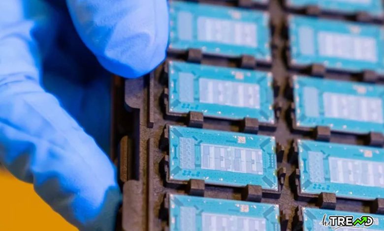
Key steps in manufacturing glass substrates include creating through-glass vias (TGV), wet etching, automated optical inspection, sputtering, ABF lamination, and precision cutting of the massive 515mm x 510mm panels. All of these processes are handled by the coalition partners.
Among these processes, E&R has overcome a significant bottleneck in the crucial TGV laser drilling step. The press release notes that while glass substrates have been around for over a decade, throughput was previously abysmal at just 10-50 vias per second.
However, after five years of collaboration
with an unnamed North American IDM customer, E&R has made a major breakthrough. They’ve achieved a throughput of 8,000 vias per second for fixed layouts and 600-1,000 vias per second for custom designs, all with tight accuracy within industry standards. This advancement makes glass substrates viable for mass manufacturing.Industry coalition aims to make glass substrates the standard in chipmaking
The company plans to showcase its latest glass manufacturing solutions at SEMICON Taiwan and SEMICON Europa later this year.
Beyond E&R, major chipmaking companies such as TSMC, Intel, Samsung Electronics, and Huawei are also investing heavily in R&D for glass substrates. Samsung aims to incorporate these substrates into commercial products by 2030.
Follow HiTrend on X