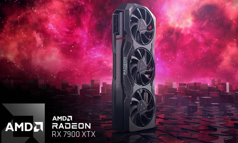
AMD patent unveils multi-chiplet GPU

According to the official Hitrend website of the technology department , Chipmakers are getting serious about splitting up complex chip designs across multiple smaller “chiplets.” AMD is leading the charge, having already implemented multi-chiplet architectures for its CPUs and data center GPUs. The company’s latest RDNA 3 PC graphics cards even incorporate basic chiplets. However, a new patent filing shows these designs have not realized their full potential.
The December 2022 patent describes a GPU design split across multiple GPU chiplet sets. Each chiplet has a frontend die paired with several other shader-engine dies. The clever part is that these GPU chiplets can flexibly combine in various configurations.
For instance, chiplet sets can work together as a single, unified GPU, operating like a traditional monolithic GPU design–or AMD can split the sets into distinct groups, each functioning as an independent GPU. There’s even a hybrid mode where some chiplet sets act as a unified GPU while others operate independently.
This modular GPU design has several benefits. For one, it allows scaling up or down GPU resources and performance based on product needs or operating modes.
“By dividing the GPU into multiple GPU chiplets, the processing system flexibly and cost-effectively configures an amount of active GPU physical resources based on an operating mode. In addition, a configurable number of GPU chiplets are assembled into a single GPU, such that multiple different GPUs having different numbers of GPU chiplets can be assembled using a small number of tape-outs and a multiple-die GPU can be constructed out of GPU chiplets that implement varying generations of technology.”
This chiplet design could also offer cost optimizations by using different dies produced on a mix of process nodes. Only the most critical components, like shader cores, need to be fabbed on expensive leading-edge process technologies. The supporting frontend logic could live on cheaper, older silicon.
Of course, AMD has already adopted rudimentary versions of this chiplet philosophy for their current RDNA 3 GPUs. However, those are relatively simple designs using two types of chiplets – a primary GPU die, and memory cache dies. Rumors indicate that Nvidia is working on chiplets for the compute GPUs in its upcoming GeForce RTX 5000 series.
However, the patent looks to take things further by enabling various chiplet combinations and configurations. It’s unclear exactly when or where we might see this patent turn into reality–not all patents see the light of day. Still, it aligns with recent industry trends that point to a transition to disaggregated chip designs. Red Team has experimented with other unique chiplet designs. A newer patent filed in August 2023 describes a multi-die GPU design with no central processor directing the various chiplets.


Not Core 2 Duo but Pentium Pro. Some disagree but since they too agree that Nehemiah is Pentium Pro based and Sandy Bridge is on high level almost identical to Nehemiah, we can say Raptor Lake is indeed based on Pentium Pro. There just are not single totally new architecture between Pentium Pro and Raptor Lake.